4D Mercury CV Application Chart
https://4dimensions.com/application-chart
Click here 
Mercury Probe C-V map Systems:
Measurement techniques Capacitance-Voltage (CV):
- Cd (square wave deep pulse)
- Cq (square wave quasi static)
- Ch (square wave high frequency)
- Sinusoidal Ch (Agilent 4192A, 4285 A, Keithley 590)
Current Voltage
- Current range 10fA to 1mA, Voltage range up to +/-100V
- Extended Voltage range +/- 1000V (Keithley 2410, 237)
- Constant current
- Constant voltage
- Multi-terminal IV curves (pseudo MOST technique)
Silicon Oxide And Gate Material, Characterization And Integrity Monitoring:
- Cox (Oxide capacitance)
- tox (Oxide thickness)
- K value (dielectric constant)
- K-f (frequency dependent dielectric constant)
- teq (equivalent oxide thickness)
- Vfb (flat band voltage)
- Dit (Interface trap density)
- (Sheet) Resistance and Resistivity measurement of SiO2 and semi-insulating materials
- TDDB (Time dependent dielectric breakdown) tests:
- tbd (time to breakdown)
- Qbd (Charge to Breakdown)
- Vbd (ramp breakdown Voltage)
- Defect density (Density of defect causing early breakdown, e.g. Pinhole density)
- Cumulative
Compound Semiconductors
- N(W) Carrier density profiling
- Resistivity of semi-insulating substrates or layers
- Pinch-off Voltage
High Resistivity Materials
- I-V (Current vs. Voltage)
- (Sheet) Resistance and Resistivity measurement
Ferroelectric materials
- K-E (dielectric vs. electric field)
- P-E (polarization vs. electric field)
- K-f (dielectric vs. frequency) with Model 192 probe station
- K-T (dielectric vs. temperature) with temperature chamber for Tc (Curie temperature)
- Hysteresis loop
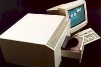
CVmap 92A/B
https://4dimensions.com/c-v%2Fi-v-c-v-map-series
Click here
Mercury Probe Systems CVMAP 92 A/B
- Desktop system
- Unique Mercury probe:
- Dot area 5E-5 to 0.6 cm2
- Contact area repeatability better 2%
- Contact configurations: Dot, Dot / Ring, Dot / 2 Rings
- Refreshed mercury before each contact insures clean contact
- Probe head easy to change
- Integrated light source for illumination of measured sample (probe head dependent)
- Minimal probe head to wafer contact area
- Non scratching poly-carbonate probe head material
- Capacitance test:
- Quasistatic method with square wave signals (internal)
- High frequency method with square wave signals (internal)
- Deep pulsed method with square wave signals (internal)
- Test frequency up to 10kHz (Bandwidth 1 MHz)
- External C-V meters (Bandwidth:1MHz standard, up to 10MHz optional)
- Capacitance measurement range: 0 to 20 nF
- Stray capacitance < 1.5pF (desktop systems)
- Equivalent oxide thickness by C-V: 1 nm to 2000 nm, repeatability <±1%
- Bias voltage +/- 100 V
- Current / Voltage test:
- Bias voltage +/- 100 V (with external source up to +/- 1000V, optional)
- Current range: 10fA to 1mA with freely selectable threshold
- Oxide thickness by I-V method 1.5 nm to 3nm
- Edge exclusion down to 2mm (probe head dependent)
- Versatility:
- Connections for external 2 and 4 terminal meters
- Connections for attaching external probe stage
- Internal automatic calibration
- Norms and standards:
- SEMI S2-0200 standard compliant (92A/B)
- CE mark (European models only)
- EN55024:1998
- FCC Part 15 Class A
- Up to 200 mm (8") capability
- Drawer for receiving the wafer
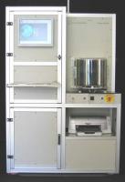
CVmap 3093AC/BC
https://4dimensions.com/c-v%2Fi-v-c-v-map-series
Click here
CVmap 3093 AC/BC Features:
- Cassette to cassette version of CVmap 3093 A/B
- 150mm, 200 mm, and 300 mm (6", 8", and 12") capability
- Safety first design principle
- Unique Mercury probe:
- Dot area 5E-5 to 0.6 cm2
- Contact area repeatability better 2%
- Contact configurations: Dot, Dot / Ring, Dot / 2 Rings
- Refreshed mercury before each contact insures clean contact
- Probe head easy to change
- Integrated light source for illumination of measured sample (probe head dependent)
- Minimal probe head to wafer contact area
- Non scratching poly-carbonate probe head material
- Capacitance test:
- Quasistatic method with square wave signals (internal)
- High frequency method with square wave signals (internal)
- Deep pulsed method with square wave signals (internal)
- Test frequency up to 10kHz (Bandwidth 1 MHz)
- External C-V meters (Bandwidth:1MHz standard, up to 10MHz optional)
- Capacitance measurement range: 0 to 20 nF
- Stray capacitance < 1.5pF (desktop systems)
- Equivalent oxide thickness by C-V: 1 nm to 2000 nm, repeatability <±1%
- Bias voltage +/- 100 V
- Current / Voltage test:
- Bias voltage +/- 100 V (with external source up to +/- 1000V, optional)
- Current range: 10fA to 1mA with freely selectable threshold
- Oxide thickness by I-V method 1.5 nm to 3nm
- Edge exclusion down to 2mm (probe head dependent)
- Versatility:
- Connections for external 2 and 4 terminal meters
- Connections for attaching external probe stage
- Internal automatic calibration